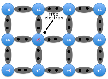
Energy Bands in SolidsElectrons in free atoms have discrete energy values. In contrast, the energy states available to the free electrons in a metal sample form a continuum of “energy bands.” In the atomic lattice of a substance, there is a set of filled atomic energy “bands” with a full complement of electrons, and a set of higher energy unfilled “bands” which have no electrons. The highest energy band contains valence electrons available for chemical reactions. The conduction band is the band above the valence band. Electrons in the conduction band are free to move about in the lattice and can conduct current. In order for a substance to conduct electricity, its valence electrons must cross the band gap, which is the energy gap between the valence band and conduction band.  If the gap between the valence and conduction bands is large, then the substance does not conduct electricity easily (it is an insulator). On the other hand, these bands overlap in metallic samples, which make these samples excellent conductors of electricity. In the case of semiconductors, the gap is small enough for electrons to jump to the conduction band due to thermal or some other excitation.  Because the band gap is so small for semiconductors, doping with small amounts of impurities can dramatically increase the conductivity of the material. Doping, therefore, allows scientists to exploit the properties of sets of elements referred to as “dopants” in order to modulate the conductivity of a semiconductor. What is Semiconductor ? Semiconductors are materials which have a conductivity between conductors (generally metals) and nonconductors or insulators (such as most ceramics). Semiconductors can be pure elements, such as silicon or germanium, or compounds such as gallium arsenide or cadmium selenide. In a process called doping, small amounts of impurities are added to pure semiconductors causing large changes in the conductivity of the material. Semiconductor DopingThere are two types of dopants, n-type (“n” for negative), and p-type (“p” for positive) dopants. n-type dopants act as electron donors and have extra valence electrons with energies very close to the conduction band. When incorporated into the atomic lattice of a semiconductor, the valence electrons of n-type dopants can be easily excited to the conduction band. p-type dopants assist in conduction by accepting electrons. When a p-type dopant is incorporated into the atomic lattice of a semiconductor, it is able to host electrons from the conduction band, allowing the easy formation of positive holes. Generating an n-Type SemiconductorIn addition to replacing one of the lattice atoms with a group 3 atom we can also replace it by an atom with five valance electrons, such as the Group 5 atoms arsenic(As) or Phosphorus(P). In this case the impurity adds five valence electrons to the lattice where it can only hold four. This means that there is now one excess electron in the lattice(see figure below). Because it donates an electron a group 5 impurity is called a donor. Note that the material remains electrically neutral.
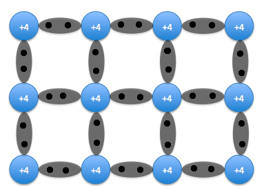
A semiconductor doped with a donor. A free electron is now present. Donor impurities donate negatively charged electrons to the lattice, so a semiconductor that has been doped with a donor is called an n-type semiconductor; "n" stands for negative. Free electrons outnumber holes in an n-type material, so the electrons are the majority carriers and holes are the minority carriers.  Generating a p-Type SemiconductorIn a pure (intrinsic) Si or Ge semiconductor, each nucleus uses its four valence electrons to form four covalent bonds with its neighbors (see figure below). Each ionic core, consisting of the nucleus and non-valent electrons, has a net charge of +4, and is surrounded by 4 valence electrons. Since there are no excess electrons or holes In this case, the number of electrons and holes present at any given time will always be equal.
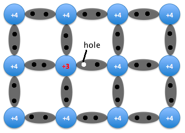
An intrinsic semiconductor. Note each +4 ion is surrounded by four electrons. Now, if one of the atoms in the semiconductor lattice is replaced by an element with three valence electrons, such as a Group 3 element like Boron (B) or Gallium (Ga), the electron-hole balance will be changed. This impurity will only be able to contribute three valence electrons to the lattice, therefore leaving one excess hole (see figure below). Since holes will "accept" free electrons, a Group 3 impurity is also called an acceptor.
A semiconductor doped with an acceptor. An excess hole is now present. Because an acceptor donates excess holes, which are considered to be positively charged, a semiconductor that has been doped with an acceptor is called a p-type semiconductor; "p" stands for positive. Notice that the material as a whole remains electrically neutral. In a p-type semiconductor, current is largely carried by the holes, which outnumber the free electrons. In this case, the holes are the majority carriers, while the electrons are the minority carriers.  |


No comments:
Post a Comment